
Principles and Applications of Semiconductor CMOS Fabrication Technology
Main Keyword: Semiconductor CMOS Fabrication
- Semiconductor CMOS fabrication involves the creation of integrated circuits using complementary metal-oxide-semiconductor technology.
- This process utilizes silicon wafers as the base material for constructing transistors and other electronic components.
- The fabrication steps include layering, patterning, doping, and etching to form intricate circuitry on the wafer.
- Through precise control of these steps, manufacturers can produce highly efficient and reliable semiconductor devices.
Sure, I can help revise the second half of the content in English and provide a summary using
- tags for clearer presentation.
- Wafer preparation
- Oxidation
- Photolithography
- Doping
- Etching
- Metallization
- Overview of Semiconductor Manufacturing Process
- Introduction to CMOS Technology
- Key Innovations in CMOS Manufacturing
- Advancements in lithography, doping techniques, and material engineering
- Introduction of high-k dielectrics and metal gates for improved performance and power efficiency
- Integration of FinFET transistors for better control of leakage currents and improved electrostatics
- Enhanced Performance: Semiconductor CMOS technology enables high-speed operation and low power consumption, making it ideal for a wide range of applications, including smartphones, computers, and IoT devices.
- Miniaturization: The continual shrinking of CMOS components allows for the creation of smaller and slimmer devices without compromising on performance, leading to sleeker and more portable gadgets.
- Energy Efficiency: As semiconductor CMOS technology becomes more power-efficient, devices can function for longer periods on a single charge, reducing energy consumption and environmental impact.
- Cost-Effectiveness: With advancements in manufacturing processes, the cost of producing semiconductor CMOS components continues to decrease, making cutting-edge technology more accessible to consumers worldwide.
- Continued scaling down of transistor dimensions
- Integration of new materials and architectures
- Shift towards non-silicon materials and 3D architectures
- Use of hazardous chemicals
- High energy consumption
- Generation of electronic waste
- Development of cleaner production processes
- Recycling of materials
- Use of renewable energy sources
The principles and applications of semiconductor CMOS fabrication technology
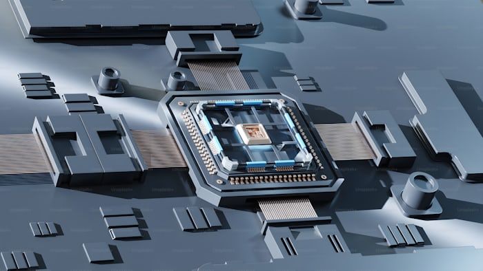
Semiconductor CMOS technology is widely used in the production of integrated circuits. It involves the fabrication of complementary metal-oxide-semiconductor transistors on a silicon substrate. The key principles of CMOS fabrication include wafer preparation, oxidation, photolithography, doping, etching, and metallization. These processes are crucial in creating the intricate patterns of transistors and interconnects on the silicon wafer.
CMOS technology offers low power consumption, high noise immunity, and scalability, making it ideal for a wide range of applications. These include microprocessors, memory chips, image sensors, and analog circuits. The ability to integrate both n-type and p-type transistors on the same chip allows for efficient logic gates and complex circuitry.
Summary:
| Application | Description |
|---|---|
| Microprocessors | Used in computing devices for processing data |
| Memory chips | Store data for electronic devices |
| Image sensors | Capture light and convert it into digital signals |
| Analog circuits | Process continuous signals for various applications |
The Basics and Innovations of Semiconductor CMOS Manufacturing Technology
Key Points:
When discussing semiconductor CMOS manufacturing technology, it is essential to understand the basics of the process as well as the innovative advancements that have shaped the industry. The manufacturing process involves intricate steps that result in the creation of complex integrated circuits. CMOS technology, which stands for Complementary Metal-Oxide-Semiconductor, plays a crucial role in the production of these circuits.
One of the key innovations in CMOS manufacturing is the development of smaller transistor sizes, allowing for greater efficiency and performance in electronic devices. Additionally, advancements in materials and production techniques have led to increased reliability and functionality of semiconductor components.
Overall, a thorough grasp of the fundamentals of semiconductor CMOS manufacturing technology, alongside awareness of the latest innovations, is vital for professionals in the field to stay at the forefront of technological advancements.
Advances in Semiconductor CMOS Manufacturing Technology
Semiconductor CMOS manufacturing technology has seen significant advancements in recent years. One key innovation is the continued scaling down of transistor sizes, leading to higher density and improved performance. This has been made possible by advancements in lithography, doping techniques, and material engineering.
Moreover, the introduction of novel materials such as high-k dielectrics and metal gates has enabled further performance enhancements while reducing power consumption. Additionally, the integration of FinFET transistors has helped to overcome some of the limitations of traditional planar CMOS technology, allowing for better control of leakage currents and improved electrostatics.
In summary, the evolution of semiconductor CMOS manufacturing technology has been driven by advancements in transistor scaling, novel materials, and innovative transistor designs such as FinFETs. These innovations have led to higher performance, lower power consumption, and improved reliability in modern semiconductor devices.
Development and Future of Semiconductor CMOS Manufacturing Technology
Main Keyword: Semiconductor CMOS
The development of semiconductor CMOS manufacturing technology has revolutionized the electronics industry, paving the way for smaller, faster, and more efficient devices. As we look towards the future, continued advancements in CMOS technology hold the key to further enhancing performance and driving innovation in various sectors.
| Year | Development |
|---|---|
| 1963 | First CMOS IC patented by Frank Wanlass |
| 1980s | CMOS technology widely adopted in the semiconductor industry |
| Present | Ongoing advancements in CMOS technology for improved performance |
The development and future of semiconductor CMOS manufacturing technology are crucial in driving advancements in various industries. One of the key areas of focus is the continued scaling down of transistor dimensions to enhance performance and reduce power consumption.
In addition to size reduction, there is a growing emphasis on the integration of new materials and architectures to improve the overall functionality of CMOS devices. The shift towards non-silicon materials and 3D architectures is poised to open up new possibilities for nanoelectronics applications.
Environmental Impact and Sustainability of Semiconductor CMOS Manufacturing Technology
Introduction:
Semiconductor CMOS manufacturing technology plays a crucial role in the production of electronic devices. However, the environmental impact of this process and its sustainability have become major concerns in recent years.
Environmental Impact:
1. Energy Consumption: The manufacturing of semiconductor CMOS devices requires a significant amount of energy, leading to greenhouse gas emissions.
2. Chemical Usage: Various chemicals are used in the fabrication process, posing risks to both human health and the environment.
3. Waste Generation: The production of semiconductor devices results in the generation of large amounts of waste, including toxic materials.
Sustainability:
1. Green Initiatives: Companies are increasingly adopting sustainable practices, such as recycling and using renewable energy sources, to reduce their environmental footprint.
2. Research and Development: Ongoing research is focused on developing more eco-friendly manufacturing processes and materials for semiconductor production.
Conclusion:
The semiconductor industry must continue to prioritize environmental sustainability to mitigate the negative impact of CMOS manufacturing technology on the environment. Companies and researchers need to work together to develop innovative solutions that promote a greener and more sustainable future for the industry.Environmental Impact and Sustainability of Semiconductor CMOS Manufacturing Technology
Semiconductor CMOS manufacturing technology has a significant environmental impact due to the use of hazardous chemicals, high energy consumption, and generation of electronic waste. However, efforts are being made to improve sustainability in this industry through the development of cleaner production processes, recycling of materials, and the use of renewable energy sources.
Key Environmental Impacts:
Efforts Towards Sustainability:
이 포스팅은 쿠팡파트너스 활동의 일환으로, 이에 따른 일정액의 수수료를 제공받습니다.